Tunneling Atomic Force Microscopy (TUNA) extends to high resistance sample surfaces the original SPM implementation, scanning tunneling microscopy of conductive samples. TUNA measures sub-picoampere tip/sample currents through highly resistive samples.
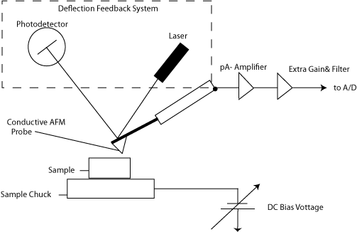
The geometry of the tip determines the lateral resolution, which is roughly equal to the end radius of the tip. With the tip at virtual ground, a selectable bias voltage is applied between the conductive tip and sample (see Figure 1). While scanning in Contact Mode, a linear amplifier with a range of 80fA to 120pA senses the current passing through the sample. By maintaining a constant force between tip and sample, simultaneous topographic and current images are generated, enabling the direct correlation of local topography with electrical properties.
TUNA is especially useful for evaluating dielectric films subject to breakdown, such as silicon dioxide, SiO2, and transistor gate oxide. Tip/sample tunneling current depends on film thickness, leakage paths, possibly caused by defects, charge traps and tip geometry. TUNA is also used to test the integrity of tribological films, such as Diamond-Like-Carbon (DLC) as used in magnetic recording head/disk interfaces, and conductivity in small structures, such as light-emitting polymers and carbon nanotubes.

Figure 1: Tunneling AFM (and Conductive AFM) Block Diagram
| www.bruker.com | Bruker Corporation |
| www.brukerafmprobes.com | 112 Robin Hill Rd. |
| nanoscaleworld.bruker-axs.com/nanoscaleworld/ | Santa Barbara, CA 93117 |
| Customer Support: (800) 873-9750 | |
| Copyright 2010, 2011. All Rights Reserved. |